
Thyristor booster device for voltage fluctuation reduction in power supply systems of ore mining enterprises
- 1 — Ph.D., Dr.Sci. Professor Nizhny Novgorod State Technical University named after R.E.Alekseev ▪ Orcid ▪ Elibrary ▪ Scopus
- 2 — Ph.D. Associate Professor Nizhny Novgorod State Technical University named after R.E.Alekseev ▪ Orcid
- 3 — Ph.D. Associate Professor Nizhny Novgorod State Technical University named after R.E.Alekseev ▪ Orcid ▪ Elibrary
- 4 — Ph.D. Associate Professor Nizhny Novgorod State Technical University named after R.E.Alekseev ▪ Orcid ▪ Elibrary
- 5 — Junior Researcher Nizhny Novgorod State Technical University named after R.E.Alekseev ▪ Orcid ▪ Elibrary
Abstract
The article is devoted to solving the problem of voltage fluctuations in the power supply systems of ore mining enterprises. The connection of high-power consumers with abruptly variable operating mode (for example, high-voltage mining excavators) causes voltage fluctuations and sags, disabling electrical equipment, communication, and automation devices in the 6-10 kV distribution network, which disrupts technological processes, etc. The use of existing solutions and methods to reduce voltage variations caused by dynamic loads is not effective. To solve the problem, booster transformers with high-speed thyristor switches can be used to work out switching the control steps towards increasing or decreasing the voltage. The authors offer a new circuitry solution for a thyristor booster device (TBD) with a pulse-phase control method. The purpose of the research is to determine the control laws of TBD, which enable to effectively reduce voltage fluctuations from dynamic load in the power supply systems of mining enterprises. The article provides a schematic diagram of the TBD and describes the principle of operation of the device. Some modes of increasing and decreasing the output voltage of the TBD, as well as the basic mode (without voltage addition) are provided. Mathematical modeling of TBD control processes was carried out and adjustment characteristics were set taking into account the load power factor. On a simulation computer model of a 6 kV electric network with a dynamic load, the verification of the adjustment characteristics of TBD obtained during mathematical modeling was carried out. Based on the research results, the laws for regulating the output voltage of TBD were established. The TBD effective control range with normal permissible limits of odd harmonics have been determined. The conducted research will make it possible to implement the device control system.
The research was conducted with the support of a Russian Science Foundation grant N 24-29-00872, https://rscf.ru/en/project/24-29-00872
Introduction
The mining industry plays an important role in the Russian economy [1]. The strategy of the Russian Federation mineral resource base development until 2035 includes the development of advanced technologies for mining, transporting and processing minerals, and building new infrastructure elements. The solution to these problems is associated with a continuous increase in the capacity of power plants and the consumption of electrical energy.
The power supply of ore mining enterprises is characterized by the consumers’ territorial dispersion [2], the continuous advancement of the mining front and the displacement of electric energy consumers [3, 4]. The connection of high-power consumers with abruptly variable operating mode (for example, megawatt mining excavators) causes voltage fluctuations which exceed permissible values in the electrical network that negatively affects other loads [5]. Thus, a malfunction in the operation of powerful elevator machines, autogenous tumbling mills and other mining loads sensitive to voltage fluctuations leads to a shutdown of the production process, accidents, etc. Therefore, the issues of developing technical solutions for high-speed devices that provide voltage variations reduction in the electrical grid of ore mining enterprises are essential.
The facilities to reduce voltage fluctuations include soft-start devices, static reactive power sources, longitudinal compensation units, twin reactors, etc. [6, 7]. It is known that the inrush current of an electric motor can exceed the rated current eight times, causing mechanical and electromagnetic shock loads on both the electric drive and the actuators [8, 9]. Soft-start devices can ensure a smooth load increase [10]. However, it is possible that the soft starters and electric motor overheating is critical with drive frequent starts and shutdowns.
Siemens Industry Inc. produces active input frequency converters (AFE – Active front end) based on IGBT transistors for dragline operation (a monobucket excavator widely used in the mining industry) [11]. Despite the fact that AFE are more resistant to grid insurges (voltage sags, fluctuations) even when operating in inverting modes, this reliability depends on the dynamic response of the rectifier control circuit [12, 13].
A distribution static compensator (D-STATCOM) [14-16] based on a voltage inverter with controlled IGBT transistors can be used to eliminate voltage fluctuations and sags. The D-STATCOM compares the shape of the linear and reference signals that provides the correct measure of compensation for a reactive power delay or advance [17]. However, IGBT transistors have a lower overload capacity compared to thyristors, so it is more appropriate to use high-speed thyristor devices in a 6-10 kV electrical grid.
A new type of mine flameproof stabilizing transformer has been developed [18] to reduce voltage fluctuations in mine power supply systems. The compensating voltage is applied to the electrical grid voltage through a compensating transformer connected in series with the power supply line. Thus, the deviation of the electrical grid voltage amplitude is restored in real time.
The Energy Equipment Company has proposed a dynamic voltage compensator (DVC), a device with double voltage conversion [19-21] and individual phase control. The DVC is built based on controlled rectifiers, through which voltage is transmitted to capacitors [22, 23]. DVC output terminals are connected to the load via an inverter unit with IGBT modules and a booster transformer with secondary winding that induces EMF to compensate voltage sags [24, 25].
An uninterruptible power system using renewable energy sources [26] and a multi-stage device for automatic switching over to a reserve source [27] is known. However, even if the power source of a mining enterprise is a sufficiently powerful power plant, additional generators are needed to maintain the required short circuit level, which increases operating costs.
A two-transformer substation with a common dual-band controlled voltage regulator [28] can be distinguished among the approaches and devices for reducing voltage fluctuations.
The devices under consideration allow to reduce voltage fluctuations. However, their significant disadvantages are the high cost and control schemes complexity. As fluctuations relate to voltage changes lasting from half a period to several seconds, it is necessary for the device to respond quickly to voltage changes for subsequent regulation. In existing electrical grids, operational voltage regulation is performed using an electromechanical on-load tap changing device (OLTC) [29, 30]. The OLTC taps switching time is about 10 s, and the device does not have time to respond to voltage fluctuations.
The authors have developed a high-speed thyristor booster device (TBD) [31], which implements the function of longitudinal regulation that allows using a voltage boost to compensate for voltage variations on the consumer's buses. The relevance of the work is due to the need to find effective and low-cost measures to improve the power supply quality of ore mining industry facilities.
The research purpose is to determine the TBD regulation laws, which allow to effectively reduce voltage fluctuations due to dynamic load in the power supply systems of ore mining enterprises.
Methods
To conduct the research, it is necessary to develop simulation math and computer models of the electrical grid with TBD and dynamic load, that allow to obtain TBD adjustment characteristics for various modes of operation of the device and load parameters. Schematic circuit diagram and equivalent circuit of the developed TBD are shown in Fig.1.
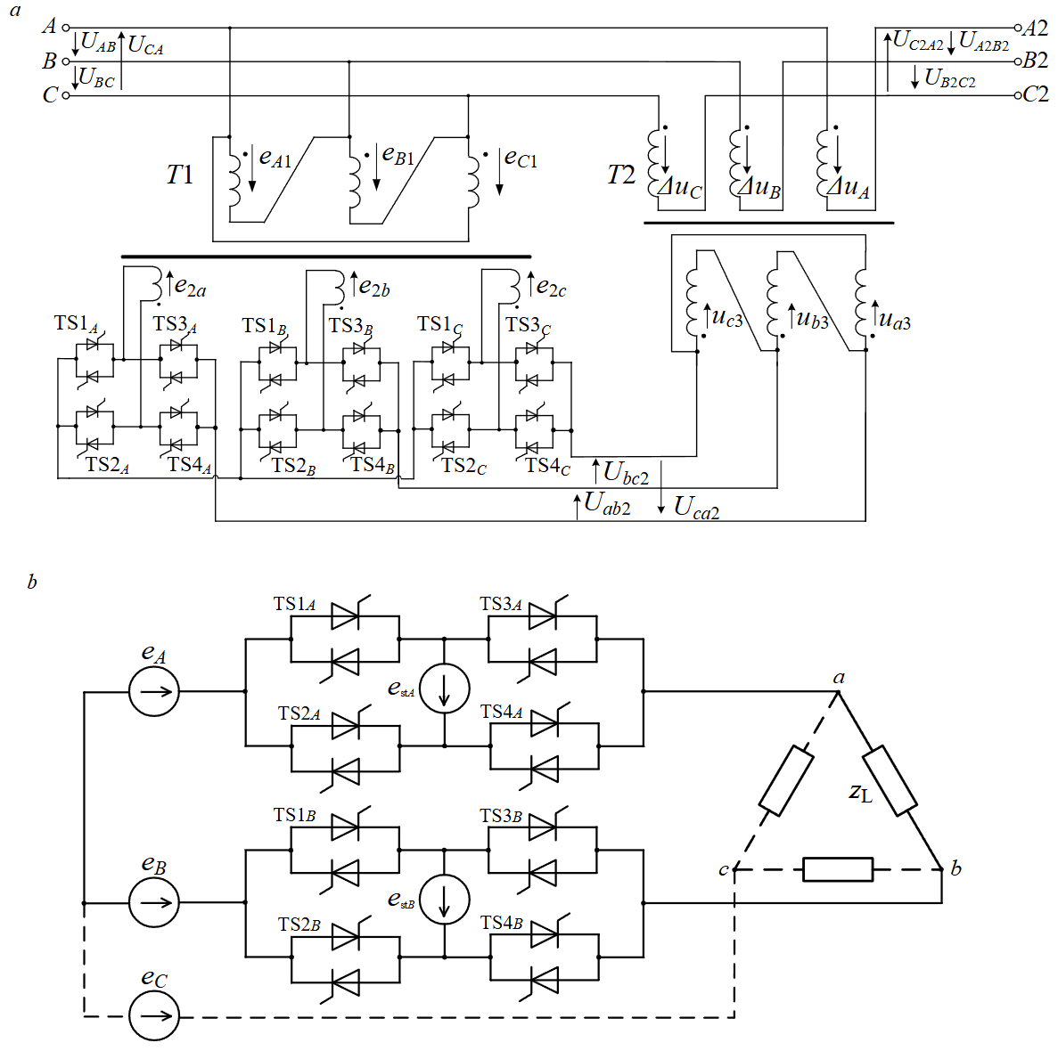
Fig.1. Thyristor booster device: a – schematic circuit diagram; b – equivalent circuit
T1, Т2 – shunt and series transformers; ТS1-ТS4 – phase A, B and C thyristor switch modules
The TBD includes a three-phase thyristor switch, three-phase shunt T1 and series T2 transformers. Each phase of the thyristor switch is a bridge converter with two-direction switches TS1-TS4 in each branch (Fig.1, а). The TBD operation principle is based on the introduction of a boost voltage when the device output voltage amplitude changes relative to the input voltage.
32 control stages are provided for the three main TBD operation modes (1 – output voltage increase; 2 – basic mode (without voltage boost); 3 – output voltage reduction): 16 steps correspond to mode 1 (0-15 steps); 16 steps correspond to mode 3 (17-32 steps); control stage 16 corresponds to basic mode 2. Each stage corresponds to definite values of thyristor control angles α1 and α2. The required block of counter-parallel thyristors is opened in each phase depending on the set mode – TS1 and TS4 for mode 1, TS2 and TS3 for mode 3. The forward conductance mode (basic) corresponds to the opening of counter-parallel thyristors blocks TS2 and TS4. The time of one TBD switching is about 20 ms, the maximum switching time of all 32 control stages is 1 s.
EMF of control stage est is added in mode 1, when it is necessary to increase the voltage level on the load buses:
where UL and Ug are the load and electrical grid RMS voltage.
EMF of control stage est excluded from the current circuit in mode 2 (basic).
In mode 3, if the voltage level on the load needs to be reduced, the following equation is true:
Two-zone control is provided: the conversion from mode 1 to mode 2 is carried out by increasing the thyristors control angle α1 from 0 to 180° with a constant value of the control angle α2 = 180°, and then decreasing α2 from 180 to 0° with a constant α1 = 180°. The same alternating two-zone control is used for a smooth conversion from mode 3 to mode 2.
The TBD control system includes active adaptive algorithms that allow the device to operate in automatic mode. TBD thyristors are controlled in a phase-pulse method, ensuring the accuracy and efficiency of voltage regulation [32]. The current sensors application is not required, that preserve the TBD control properties while responding promptly to load currents changes.
The line voltage (there is no neutral wire) is regulated in 6-10 kV electrical grid, using the TBD. The TBD operation principle is considered using the example of line voltage regulation UAB: ТS1A, ТS4A, ТS1B, ТS4B are activate in mode 1; ТS2A, ТS4A, ТS2B, ТS4B – in mode 2; ТS2A, ТS3A, ТS2B, ТS3B – in mode 3.
The advantages of TBD over thyristor regulators [33, 34] are a reduced number of thyristor switch modules and reduced transformer power (that increases the device reliability and safety), as well as less distortion of the output voltage curve.
Math and computer simulation of TBD increasing and decreasing voltage modes, taking into account the load parameters, enable to determine regulation laws which will form the basis of the device control system in the electrical grid.
Math simulation of TBD operation modes
The laws of load voltage change (phase and linear) when TBD switching from mode 1 or 3 to basic mode 2 by alternating changing the thyristor control angles α1 (in the intervals of the positive power direction) and α2 (in the intervals of the negative power direction) are described in detail in [35]. An example of diagrams of voltage changes is shown in Fig.2 when the TBD is switched from mode 1 to mode 2 by alternating changing the angles α1 (Fig.2, а) and α2 (Fig.2, b).
Due to TBD operation analysis based on the diagrams, it is possible to describe mathematically the processes of TBD output voltage regulation and determine the main parameters, that affect the behavior of the device adjustment characteristics, i.e., it is possible to identify the dependence of RMS output voltage on the control voltage Ucont at different load angles.

Fig.2. Load instantaneous phase and line voltage in TBD mode 1 on change α1 (а) and α2 (b)
Math equations describing the adjustment characteristics were obtained using the method of alignment boundary values [36, 37]. The method allows to describe processes in piecewise-linear systems. The integration constants are determined by conjugating equations at the boundaries of adjacent intervals in each time interval, using the first and second switching laws (conditions for continuity of current in inductive elements and voltage across capacitors) at the switching moments. The Accepted assumptions are: the resistance of the magnetic circuit and winding T2 is not taken into account (Fig.1, a); the load is active-inductive, linear. The amplitude of the electrical grid phase voltage is taken as the basic value.
Instantaneous values of phase voltages on the load side are obtained based on the analysis of TBD modes 1 and 3, according to the diagrams. The instantaneous values of the line voltage of the load, which connected between A and B phases, are determined by the formula
where are the load instantaneous voltages on phase А and В, a.u.
The RMS load voltage are calculated using the formula
where is a load line voltage, a.u.
The conversion of TBD from modes 1 and 3 to mode 2 in the effective variation intervals α1 and α2 is considered. Effective intervals are intervals that provide a significant change in the shape and amplitude of the voltage.
TBD mode 1 in the range of increasing α1 from 0 to 180° while α2 = 180° = const
It can be seen from the diagram (Fig.2, a) that the change in the line load voltage during the half-cycle can be divided into four ranges: ; ; ; . Instantaneous values of phase and line voltages on the load side are obtained for all ranges (1).
Instantaneous value of the line voltage:
- for the first range
- for the second range
- for the third range
- for the fourth range
The law of regulation of RMS output voltage according to the equation (2):
Similarly, equations are obtained for TBD mode 1 in the range of effective variation α2; for mode 3 in the ranges of effective variation α1 and α2.
TBD mode 1 in the range of reduction α2 from 180 to 0° while α1 = 180° = const
Changes of the load line voltage (Fig.2, b) during the half-cycle are divided into four ranges: ; ; .
Instantaneous value of the line voltage:
- for the first range
- for the second range
- for the third range
- for the fourth range
RMS load voltage
TBD mode 3 in the range of reduction α1 from 180 to 0° while α2 = 180° = const
Changes of the load line voltage are divided into four ranges during the half-cycle, according to [35]: from 0 to α1; from α1 to ; from to ; from to π.
Instantaneous value of the line voltage:
- for the first range
- for the second range
- for the third range
- for the fourth range
RMS load voltage
TBD mode 3 in the range of reduction α2 from 180 tо 0° while α1 = 180° = const
Changes of the load line voltage are divided into ranges during the half-cycle, according to [35]: from φL to α2; from α2 to ; from to ; from to π + φL.
Instantaneous value of the line voltage:
- for the first range
- for the second range
- for the third range
- for the fourth range
RMS load voltage
The analysis of the control laws (3)-(6) indicates the influence of the load phase angle φL, the control angles α1 and α2 and the depth of the control stage kst on the TBD RMS output voltage.
The control angles α1 and α2 depend on the control voltage Ucont with range from 0 to 2. Thus, the TBD RMS output voltage also depends on the Ucont. The amplitude of the reference sawtooth voltage of the phase-pulse control circuit is taken as the base value. At the same time, thyristor switching pulses are formed at the moments when the control voltage and the reference voltage are equal.
The TBD adjustment characteristics in modes 1 and 3 at φL = 0°, 30° and 60° are determined according to equations (3)-(6). The graphs are constructed at the depth of the control stage kst = 0.1 and electrical grid voltage U = 6,000 V.
Computer simulation
A computer simulation model of a 6-10 kV electrical grid section was developed in the Matlab (Simulink) simulation environment, and it enables to verify and refine the TBD adjustment characteristics obtained during the math simulation. Both existing elements of the SimPowerSystems library and masked blocks missing from the standard library are used in the model. The high calculation accuracy and high performance of the TBD model are due to a two-step approach to solving differential equations (the ode23tb method was used for the solution). The Runge – Kutta method is used at the first stage, and the method based on the second – order inverse differentiation formulas is used at the second stage.
Rated load power SL = 630 kV·А. The power regulated in the developed TBD model when changing the angle of shift of the main harmonic of the output voltage relative to the input voltage in the range of ± 5° and regulation the output voltage in the range of ±14 % is ~20 % of the load power. The passport values of device power elements (transformers, thyristors, etc.) are entered in the block of parameters of the TBD model elements to simulate the operation of the device in real conditions.
Fig.3 shows a block diagram of the electrical grid section computer simulation model with the TBD.
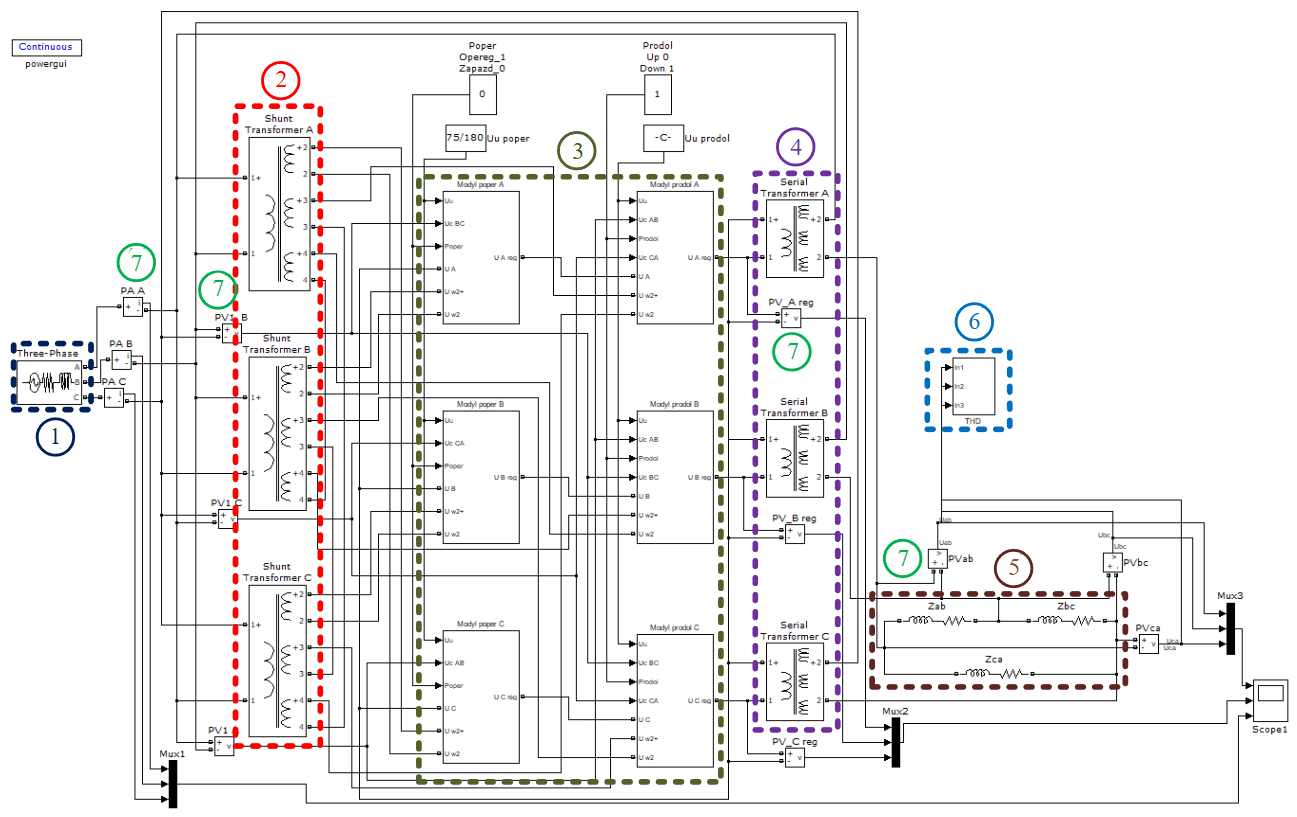
Fig.3. Simulation model of electrical grid section with TBD
1 – three-phase power supply block (U = 6 kV; f = 50 Hz; R = 0.231 Ohm; L = 0.00368 H); 2 – shunt transformer block (S = 106 kV·А); 3 – thyristor switches module; 4 – series transformers block (S = 3×28 kV·А); 5 – electrical load block (U = 6 kV; S = 630 kV·А); 6 – higher harmonics measuring block (Fourier transform); 7 – measuring instruments
The computer simulation model includes seven main blocks: a power source (three-phase voltage source); three single-phase shunt transformers; three TBD single-phase longitudinal regulation mo-dules; three single-phase series transformers; three-phase electric load; measuring instruments (oscilloscope, ammeters and voltmeters); a three-phase measuring block of the TBD output line voltage parameters.
Voltages that are either in phase with or out of phase with the corresponding phase voltages, are generated at the output terminal of TBD. Mode 1 is implemented when the specified voltages are in phase, and mode 3 is implemented, if the specified voltages are out of phase. A three-channel oscilloscope is used for visual control of input currents, output voltages and EMFs introduced by TBD into the electrical grid. The TBD adjustment characteristics (RMS voltages) in modes 1 and 3 for different load angles are constructed using the computer simulation model.
Discussion of results
The research of the TBD adjustment characteristics obtained on the basis of the math and computer simulation under different device operating modes and load parameters allowed to determine TBD regulation laws for the control system when it is integrated into the electrical grid. Examples of TBD adjustment characteristics in mode 1 as part of the electrical grid obtained by math and computer simulation are shown in Fig.4.
An analysis of the computer simulation graphs showed that the boost voltage is 551 V (9.4 %) in the voltage increasing mode. The amplitude of the RMS output voltage is reduced by 590 V (i.e. by 10 %) in the output voltage reduction mode. The load angle influences the behavior of the TBD adjustment characteristics in both modes.
Effective change of the thyristor control angles α1 and α2 to change (Fig.4) the load voltage is in following ranges:
A comparison of the math and computer simulation TBD adjustment characteristics showed a coincidence of their character and shape (Fig.5). The computer simulation dependencies are lower than math simulation dependencies. It is explained by taking into account the voltage drops in the power supply line and on the TBD power elements, as well as taking into account the switching ranges where boost voltage value is zero. The largest deviation of the characteristics δ is observed for mode 1 at φ = 60° and is 3.5 %.
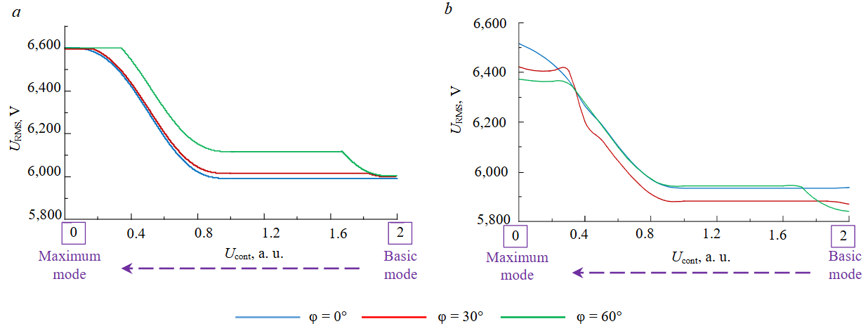
Fig.4. Adjustment characteristics of TBD in mode 1 as electrical grid part, obtained by math (а) and computer simulation (b)
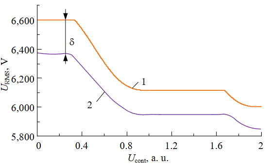
Fig.5. Adjustment characteristics for the voltage boost mode at φ = 60°: 1 – math simulation; 2 – computer simulation
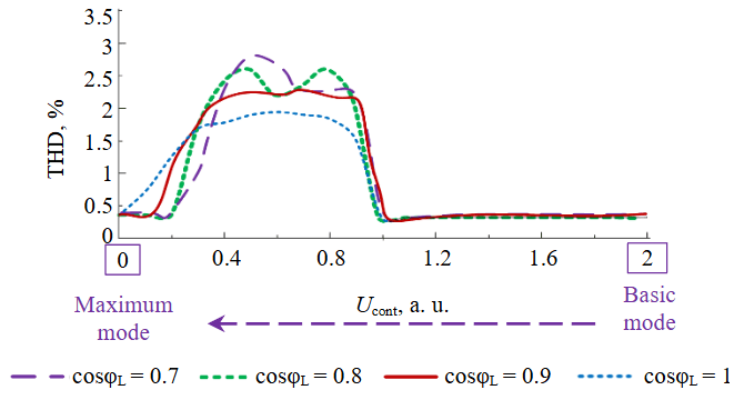
Fig.6. Graph of the total harmonic distortion of the TBD output voltage dependence in the voltage boost mode
Odd harmonics are generated in the electrical grid with the phase-pulse control method for TBD thyristors. The values of these harmonics do not exceed the allowable limits. Computer simulation allowed to obtain graphs of the change in the total harmonic distortion THD of the TBD output voltage in modes 1 and 3. An example of the TBD output voltage THD graph in mode 1 at different load power factors (cosφL) is shown in Fig.6.
It can be seen from Fig.6 that TBD output voltage THD is inversely proportional to the load power factor, i.e. THD increases with a cosφL reduction. THD takes the lowest value at active load (cosφL = 1).
Conclusion
As a result of the conducted research, the TBD regulation laws that allow to reduce voltage fluctuations by adding a voltage boost to the electrical grid have been obtained. The regulation laws represent the dependences of the TBD RMS output voltage on the load phase angle φL, the depth of the voltage step regulation kst, control angles α1 and α2. The required stage of regulation Ucont is automatically selected depending on the magnitude of the voltage variation.
The Equations of the TBD regulation laws allowed us to obtain the TBD adjustment characteristics. Depending on the control voltage, the limits of RMS output voltage regulation were ±10 %. The TBD thyristors phase-pulse control method ensures a smooth change in the output voltage. At the same time sine voltage total harmonic distortion coefficient over the entire range of effective control zones is within the range of acceptable values set by State standard 32144-2013.
The introduction of the TBD into the electrical grid of the ore mining enterprises will improve the reliability of power supply and increase the capacity of power transmission lines.
References
- Andreev D.V. Role of the mining industry in the economy of the country. Moscow Economic Journal. 2020. N 12, p. 175-185 (in Russian). DOI: 10.24411/2413-046X-2020-10870
- Nazarychev A.N., Ustinov D.A., Pelenev D.N., Babyr K.V. Studying the Single-Phase Earth Fault Protection Based on Measuring the Negative-Sequence Current. Elektrichestvo. 2024. N 2, p. 31-41 (in Russian). DOI: 10.24160/0013-5380-2024-2-31-41
- Skamyin A.N., Dobush V.S., Jopri M.H. Determination of the grid impedance in power consumption modes with harmonics. Journal of Mining Institute. 2023. Vol. 261. p. 443-454. DOI: 10.31897/PMI.2023.25
- Abdallah W.J., Hashmi K., Faiz M.T. et al. A Novel Control Method for Active Power Sharing in Renewable-Energy-Based Micro Distribution Networks. Sustainability. 2023. Vol. 15. Iss. 2. N 1579. DOI: 10.3390/su15021579
- Yaghoobi J., Abdullah A., Kumar D. et al. Power Quality Issues of Distorted and Weak Distribution Networks in Mining Industry: A Review. IEEE Access. 2019. Vol. 7, p. 162500-162518. DOI: 10.1109/ACCESS.2019.2950911
- Chun-Hsi Su, Yian-Ting Chen. A Remote-Controllable Variable Frequency Drive. Sixth International Symposium on Computer, Consumer and Control (IS3C), 30 June – 3 July 2023, Taichung, Taiwan. IEEE, 2023, p. 292-294. DOI: 10.1109/IS3C57901.2023.00084
- Tokarev I.S. Development of parameters for an industry-specific methodology for calculating the electric energy storage system for gas industry facilities. Journal of Mining Institute. 2024, p. 1-10 (Online first).
- Sinvula R., Abo-Al-Ez K.M., Kahn M.T. Harmonic Source Detection for an Industrial Mining Network with Hybrid Wind and Solar Energy Systems. Control and Operation of Grid-Connected Wind Energy Systems. Cham: Springer, 2021, p. 153-192. DOI: 10.1007/978-3-030-64336-2_7
- Le Van Tung. The structure and control algorithms for conveyors electric drive to increasing the energy efficiency of their operation in mining enterprises: Avtoref. dis. … kand. tekhn. nauk. SPb: Sankt-Peterburgskii gornyi universitet, 2021, p. 20.
- Volotkovskaya N.S., Semenov A.S., Fedorov O.V. Energy efficiency and energy saving in the power supply systems of mining enterprises. Vestnik Gomelskogo gosudarstvennogo tekhnicheskogo universiteta imeni P.O.Sukhogo. 2019. N 3, p. 52-62.
- Morán L., Espinoza J., Burgos R. Voltage regulation in mine power distribution systems: Problems and solutions. IEEE Industry Application Society Annual Meeting, 5-9 October 2014, Vancouver, BC, Canada. IEEE, 2014, p. 7. DOI: 10.1109/IAS.2014.6978453
- Sukanth T., Jayanthu S., Jayalaxmi A. Mitigation of power quality problem in underground mine using different control strategies. IEEE Region 10 Humanitarian Technology Conference (R10-HTC), 21-23 December 2016, Agra, India. IEEE, 2016, p. 4. DOI: 10.1109/R10-HTC.2016.7906798
- Serebryannikov S.V., Serebryannikov S.S., Kovalchuk V.G. et al. Electromagnetic Parameters of the Ferrite Materials for Electromagnetic Compatibility. Radiation and Scattering of Electromagnetic Waves (RSEMW), 26-30 June 2023, Divnomorskoe, Russia. IEEE, 2023, p. 316-319. DOI: 10.1109/RSEMW58451.2023.10201985
- Negi P., Pal Y., Leena G. A Review of Various Topologies and Control Schemes of DSTATCOM Implemented on Distribution Systems. Majlesi Journal of Electrical Engineering. 2017. Vol. 11. N 1, p. 25-35.
- Salkuti S.R. An efficient allocation of D-STATCOM and DG with network reconfiguration in distribution networks. International Journal of Advanced Technology and Engineering Exploration. 2022. Vol. 9. Iss. 88, p. 299-309. DOI: 10.19101/IJATEE.2021.874812
- Xuefeng Wang, Li Peng. Dynamic Voltage Equalization Control of D-STATCOM Under Unbalanced Grid Faults in a Low-Voltage Network. IEEE Transactions on Power Electronics. 2023. Vol. 38. Iss. 2, p. 2384-2397. DOI: 10.1109/TPEL.2022.3213405
- Dash S.K., Mishra S., Abdelaziz A.Y. A Critical Analysis of Modeling Aspects of D-STATCOMs for Optimal Reactive Power Compensation in Power Distribution Networks. Energies. 2022. Vol. 15. Iss. 19. N 6908. DOI: 10.3390/en15196908
- Malafeev S.I., Serebrennikov N.A. Increasing energy efficiency of mining excavators through upgrade of electrical equipment and control systems. Ugol. 2018. N 10, p. 30-35 (in Russian). DOI: 10.18796/0041-5790-2018-10-30-34
- Mohite S., Jape V.S., Bankar D.S. Power Quality Problems Mitigation by DVR Using SC Structured Cascaded MPAC. Proceedings of the 1st International Conference on Data Science, Machine Learning and Applications. Springer, 2019. Vol. 601, p. 796-804. DOI: 10.1007/978-981-15-1420-3_86
- Seershak M., Muhammed Ramees M.K.P. Power Quality Improvement Using ZSI-DVR. International Conference on Futuristic Technologies in Control Systems & Renewable Energy (ICFCR), 21-22 July 2022, Malappuram, India. IEEE, 2022, p. 6. DOI: 10.1109/ICFCR54831.2022.9893660
- Jape V.S., Kulkarni H.H., Lokhande N.M., Ubale D. Observations and Analysis of Power Quality Indices Using Custom Power Devices in Power Distribution Network. Information and Communication Technology for Competitive Strategies (ICTCS 2021), 17-18 December 2021, Rajasthan, India. Springer, 2021. Vol. 401, p. 121-130. DOI: 10.1007/978-981-19-0098-3_13
- Amarendra A., Srinivas L.R., Rao R.S. Contingency Analysis in Power System- Using UPFC and DVR Devices with RDOA. Technology and Economics of Smart Grids and Sustainable Energy. 2022. Vol. 7. Iss. 1. N 17. DOI: 10.1007/s40866-022-00129-y
- Kandil T., Ahmed M.A. Control and Operation of Dynamic Voltage Restorer With Online Regulated DC-Link Capacitor in Microgrid System. Canadian Journal of Electrical and Computer Engineering. 2020. Vol. 43. Iss. 4, p. 331-341. DOI: 10.1109/CJECE.2020.3002855
- Bakhteev K.R. Improving the efficiency of centralized and autonomous power supply systems through the integrated use of electrochemical energy storage devices, low-power generation, and forced excitation of synchronous machines: Avtoref. dis. … kand. tekhn. nauk. Kazan: Kazanskii gosudarstvennyi energeticheskii universitet, 2019, p. 24.
- Yerbayev Y., Artyukhov I., Zemtsov A. et al. Negative Impact Mitigation on the Power Supply System of a Fans Group with Frequency-Variable Drive. Energies. 2022. Vol. 15. Iss. 23. N 8858. DOI: 10.3390/en15238858
- Jahromi M.G., Mirzaeva G., Mitchell S.D., Gay D. Powering Mobile Mining Machines: DC Versus AC Power. IEEE Industry Applications Magazine. 2016. Vol. 22. Iss. 5, p. 63-72. DOI: 10.1109/MIAS.2015.2459082
- Abramovich B.N. Uninterruptible power supply system for mining industry enterprises. Journal of Mining Institute. 2018. Vol. 229, p. 31-40. DOI: 10.25515/PMI.2018.1.31
- Tabarov B.D., Solovyev V.A., Ivanov V.I. A Two-Transformer Substation with a Common Dual-Band Controlled Voltage Regulator. Elektrichestvo. 2024. N 4, p. 74-84 (in Russian). DOI: 10.24160/0013-5380-2024-4-74-84
- Hem P., Heang S., Eam D. et al. Service Restoration in Distribution Systems with a Load Tap Changer. International Electrical Engineering Congress (iEECON), 9-11 March 2022, Khon Kaen, Thailand. IEEE, 2022, p. 4. DOI: 10.1109/iEECON53204.2022.9741590
- Dyussembekova N., Schütt R., Leiße I., Ralfs B. Decision Process for Identifying Appropriate Devices for Power Transfer between Voltage Levels in Distribution Grids. Energies. 2024. Vol. 17. Iss. 9. N 2158. DOI: 10.3390/en17092158
- Asabin A.A., Sosnina E.N., Kralin A.A., Kriukov E.V., Bedretdinov R.Sh., Gusev D.A. Patent N 2813363 RF. Thyristor voltage booster device of longitudinal voltage control. Publ. 12.02.2024. Bul. N 5 (in Russian).
- Zhmurov V.P., Stelmakov V.N., Tarasov A.N., Timoshenko A.L., Kazennova I.I. Patent N 2450420 RF. Semiconductor phase shifter. Publ. 10.05.2012. Bul. N 13 (in Russian).
- Bedretdinov R.Sh., Verkhovskii S.Ya., Sosnina E.N., Kisel D.A., Asabin A.A., Gardin A.I. Patent N 157116 RF. Solid-state phase shifter device. Publ. 20.11.2015. Bul. N 32 (in Russian).
- Asabin A., Sosnina E., Belyanin I. et al. Control System of the Thyristor Voltage Regulator. 7th International Conference on Control, Decision and Information Technologies (CoDIT), 29 June – 2 July 2020, Prague, Czech Republic. IEEE, 2020, p. 802-806. DOI: 10.1109/CoDIT49905.2020.9263984
- Kryukov E.V. The use of thyristor booster devices to improve the quality of electric energy in power supply systems: Avtoref. dis. … kand. tekhn. nauk. Nizhnii Novgorod: Nizhegorodskii gosudarstvennyi tekhnicheskii universitet im. R.E.Alekseeva, 2018, p. 18.
- Belov G.A., Malinin G.V. Vector-matrix method for transients calculating in dc resonant converter of the LCL-T type. Practical power electronics. 2020. N 1 (77), p. 28-37 (in Russian).
- Umarov Sh. Comparative analysis of two methods for modeling valve converter devices. Universum: engineering science. 2023. N 11 (116), Part 6, p. 13-18 (in Russian). DOI: 10.32743/UniTech.2023.116.11.16253